
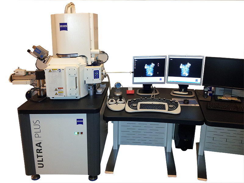
 The Laboratory possess scanning electron microscopy for morphological characterisation, chemical composition analysis.
During Scanning Electron Microscopy (SEM) investigations, a focussed electron beam scans the surface of specimens. Field Emission microscopes can reach resolution of surface topography in the range of 1 nm, while the accelerating voltage is even as low as 1 kV, so that bio-materials can be investigated as well. The electron beam excites a range of signals form the surface, permitting to observe surface morphology, phase composition, and other. For an instrument with attached EDS system, the energy of excited x-rays can be analysed and chemical composition of samples mapped.
Our services are delivered on market prices since 15 years, and our equipment is operating for the public every day. We have the ISO 17025 certificate for SEM observations of nanomaterials morphology and chemical composition.